Project: Flat and Porous Electronic Optical Device
The fabrication of such a device relies on the ability to locally control the phase of a wave transmitted through the device. In photonic optics, this control results from the realization of controlled thicknesses of a transparent material (e.g. glass) with an optical index different from the medium in which the wave propagates (e.g. air). Such a control is currently unfeasible in electronic optics or UV and X-ray photonics. In the case of electro-optical devices, phase changes are induced by the transmission of an electron wave through electromagnetic potentials produced by electrodes or coils. The structure of these potentials induces strong constraints on the realization of the devices, in particular that of working very close to the optical axis, otherwise the performance of the device will be significantly degraded.
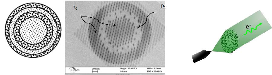
We have shown that it is possible to change the phase of an electron wave during its transmission through an ultra-thin porous film. This approach has a similarity with photonic optics where a property of a material is exploited. It is then possible to fabricate electro-optical devices or functions that rely on the phase change of an electronic wave passing through an ultra-thin film whose local porosity is controlled. This film is self-supported, of uniform thickness and thin enough to make it partially transparent to electrons. It is made of nanometric pores whose density defines the local porosity of the film. The phase of the electron wave transmitted through the film is determined by this local porosity. This innovative concept could be developed in the field of X and UV photons.