
Spintronics and Epitaxy
Our research activities are focused on the development of thin film materials and nanostructures based on metals, silicon and germanium, the most widely used semiconductor materials in electronics.
Our objective is to study the original physical properties of these objects and their integration into current electronic devices. We are particularly interested in materials and heterostructures for spin electronics -spintronics-, a branch of electronics exploiting the phenomena related to the electron spin.
Original effects related to spin-dependent electronic transport can indeed emerge from:
- the reduction of materials to the nanometer scale,
- the association of materials in a heterostructure.
The interfaces often play a key role in these structures. Thus, our activity is mainly oriented toward the study of heteroepitaxy, structural and chemical characterizations of nanostructures and existing interfaces, and the study of physical properties, particularly electrical and magnetic ones. Our main goal is to study the interplay between structure and physical properties.
The elaboration and growth of materials are mainly carried out using molecular beam epitaxy (MBE), a technique in which kinetic and thermodynamic aspects, epitaxial growth modes, and stress states in the films must be considered. The main used characterization techniques are RHEED (in situ monitoring of vacuum deposits), XRD, TEM, AFM, SQUID, VSM, etc.
The associated research topics are:
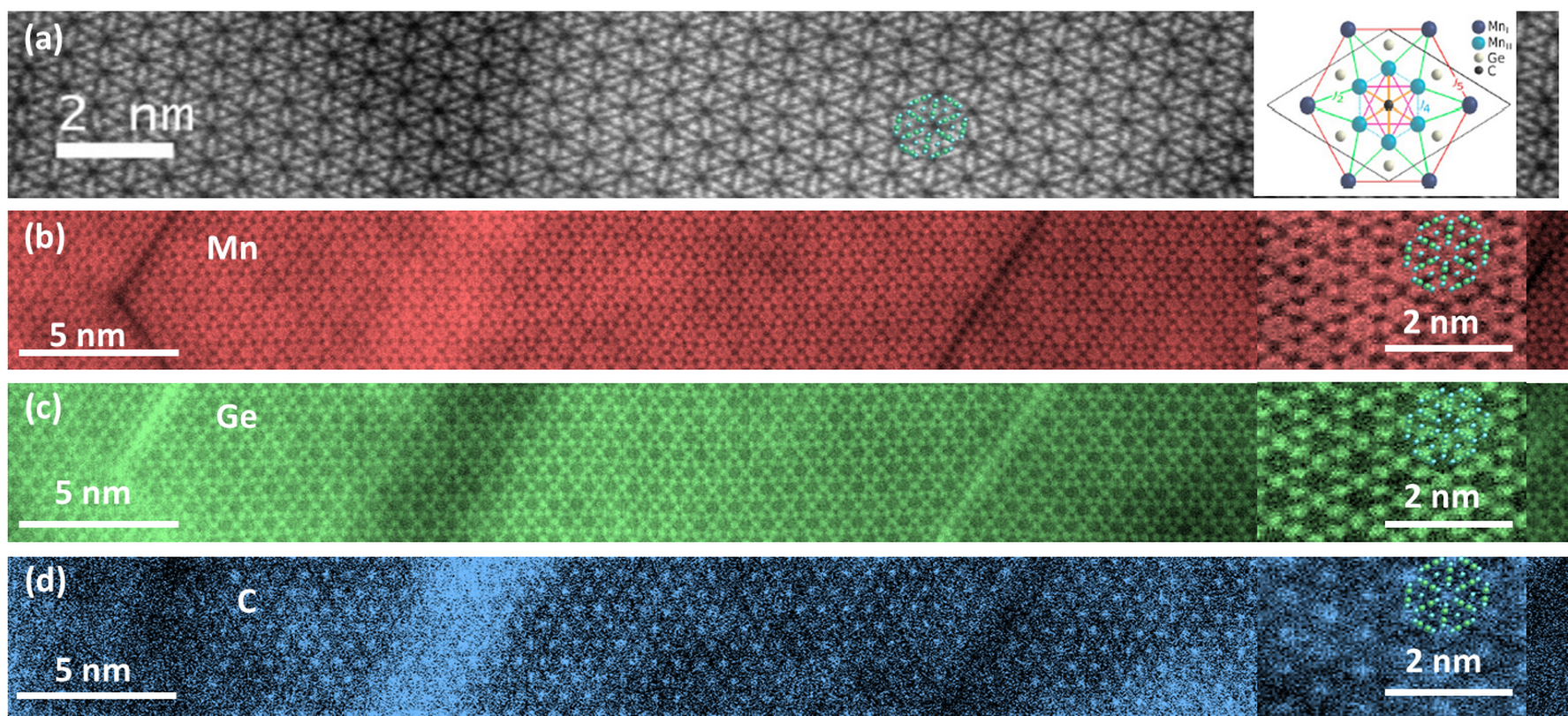
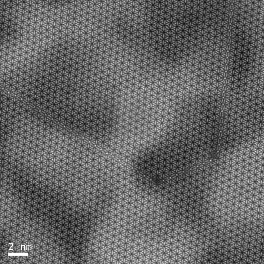
Fig.2: (a) Planar STEM image of a C dpoed Mn5Ge3 layer. Inset: unit cell of the Mn5Ge3 hexagonal lattice along the c axis. The C atom is in the octaedric interstitial site created by the type II Mn atoms.
(b), (c) et (d) Elemental map recorded by EELS showing the positions of the Mn, Ge and C atoms.
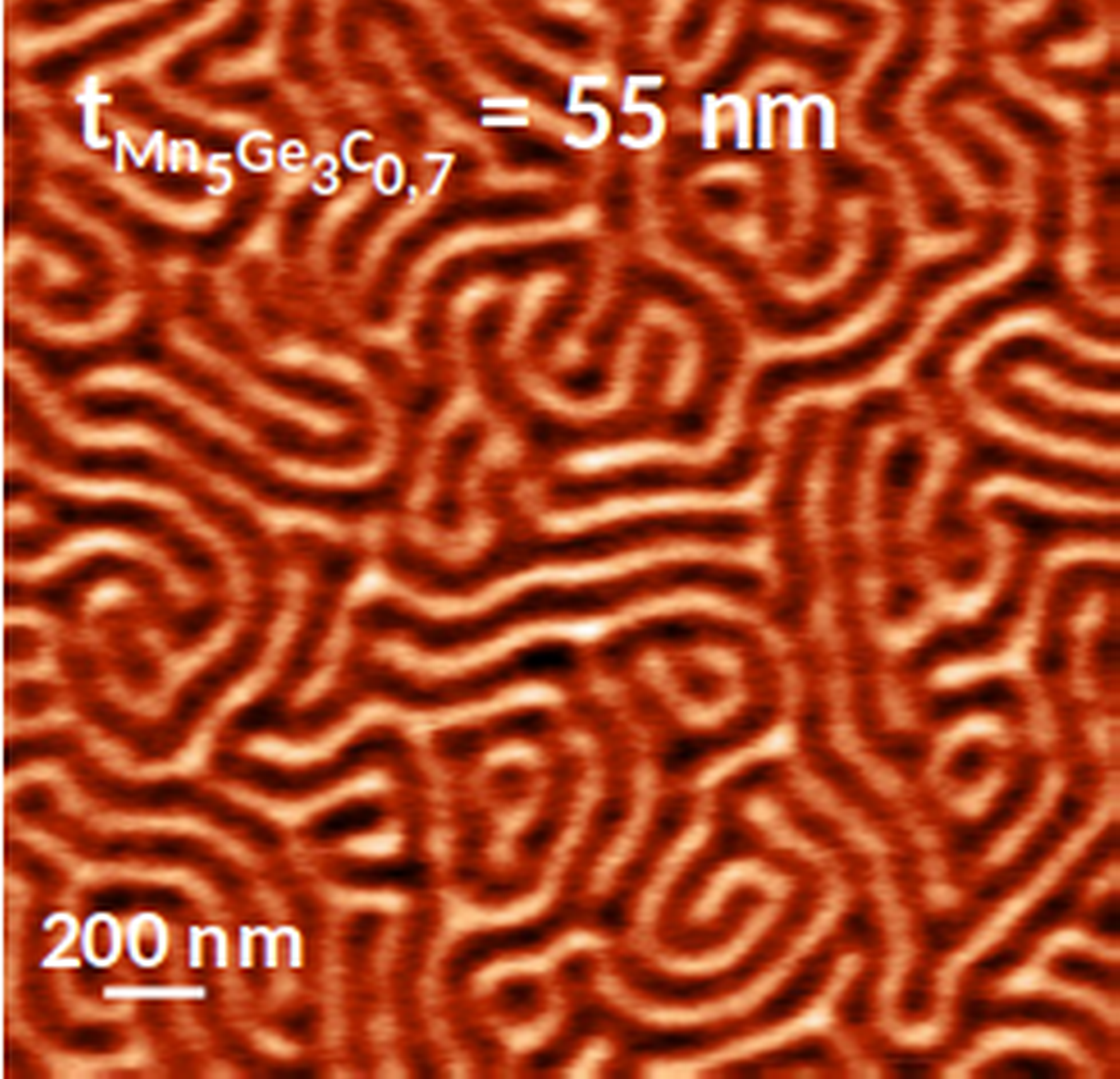
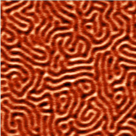
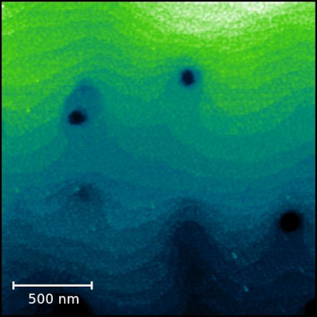
Fig. 3 :MFM image of 50 nm thick Mn5Ge3C0.5 film showing the magnetic domains structure.
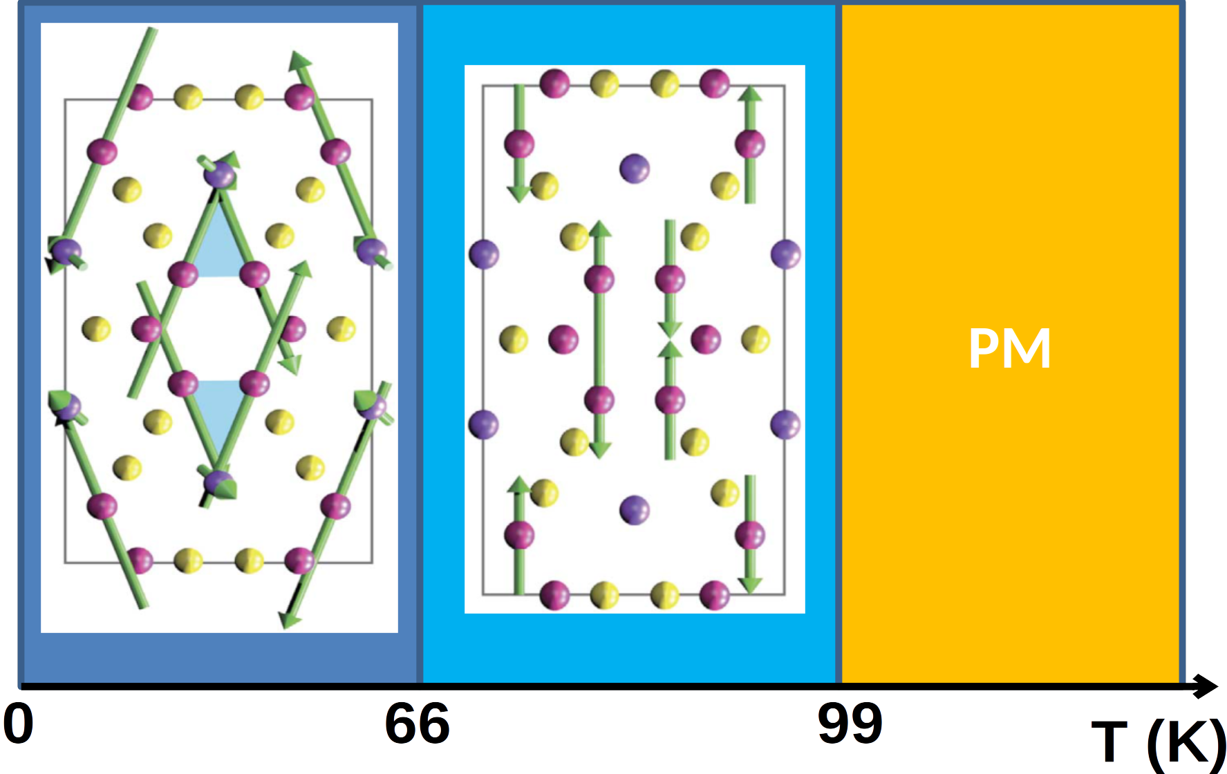
Fig. 4: Mn5Si3 is an anti-ferromagnetic materials exhibiting an anti-colinear and a colinear phases.
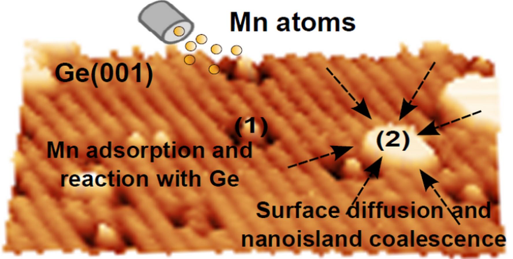
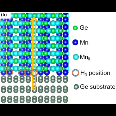
Fig. 5: First growth step of Mn on Ge(001): islands are formed between the Ge dimers by consumming the Ge atoms of the adjacents rows.
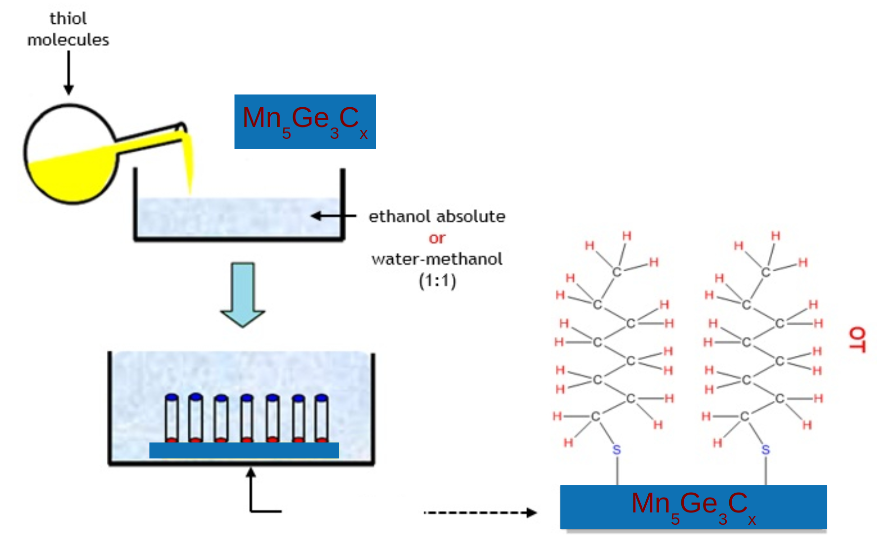
Fig. 6 :functionalization of the Mn5Ge3 surface by an octanethiol SAM.


2026
Altermagnétisme : la face cachée du monde magnétique
Vincent Baltz, Lisa Michez
Reflets de la Physique 25-31 (2026)10.1051/refdp/202683025
Magnetic aftereffect and Barkhausen effect in thin films of the altermagnetic candidate Mn5Si3
Gregor Skobjin, Javier Rial, Sebastian Beckert, Helena Reichlova, Vincent Baltz, Lisa Michez, Richard Schlitz, Michaela Lammel, Sebastian Goennenwein
Applied Physics Letters 128:102407 (2026)10.1063/5.0314005
2025
Intrinsic Magnetism and Field‐Driven Spin Alignment in NiI2 Revealed by X‐ray Magnetic Spectroscopy
Ethan L Arnold, Emily Heppell, Rabindra Basnet, Binshuo Zhang, Jieyi Liu, Javier Herrero-Martín, Charles Guillemard, Yanfeng Guo, Jin Hu, Dirk Backes, Gerrit van der Laan, Thorsten Hesjedal
physica status solidi (RRL) - Rapid Research Letters (pss RRL) (2025)10.1002/pssr.202500130
Even-in-magnetic-field part of transverse resistivity as a probe of magnetic order
Antonin Badura, Dominik Kriegner, Eva Schmoranzerová, Karel Výborný, Miina Leiviskä, Rafael Lopes Seeger, Vincent Baltz, Daniel Scheffler, Sebastian Beckert, Ismaila Kounta, Lisa Michez, Libor Šmejkal, Jairo Sinova, Sebastian Goennenwein, Jakub Železný, Helena Reichlová
Applied Physics Letters 126:172404 (2025)10.1063/5.0269699
Observation of the anomalous Nernst effect in altermagnetic candidate Mn5Si3
Antonin Badura, Warlley Campos, Venkata Bharadwaj, Ismaïla Kounta, Lisa Michez, Matthieu Petit, Javier Rial, Miina Leiviskä, Vincent Baltz, Filip Krizek, Dominik Kriegner, Jan Zemen, Sjoerd Telkamp, Sebastian Sailler, Michaela Lammel, Rodrigo Jaeschke Ubiergo, Anna Birk Hellenes, Rafael González-Hernández, Jairo Sinova, Tomáš Jungwirth, Sebastian Goennenwein, Libor Šmejkal, Helena Reichlova
Nature Communications 16:7111 (2025)10.1038/s41467-025-62331-7
Detecting slow magnetization relaxation via magnetotransport measurements based on the current-reversal method
Sebastian Beckert, Richard Schlitz, Gregor Skobjin, Antonin Badura, Miina Leiviskä, Dominik Kriegner, Daniel Scheffler, Giacomo Sala, Kamil Olejník, Lisa Michez, Vincent Baltz, Andy Thomas, Helena Reichlová, Sebastian Goennenwein
Physical Review B 111:014441 (2025)10.1103/PhysRevB.111.014441
Dissipation properties of anomalous Hall effect: Intrinsic vs extrinsic magnetic materials
V Desbuis, D Lacour, M Hehn, S Geiskopf, L Michez, J Rial, Vincent Baltz, J-E Wegrowe
Journal of Applied Physics 138:233906 (2025)10.1063/5.0281311
Unusually High Occupation of Co 3d State in Magnetic Weyl Semimetal Co 3 Sn 2 S 2
Jieyi Liu, Yiheng Yang, Jianlei Shen, Defa Liu, Gohil Singh Thakur, Charles Guillemard, Alevtina Smekhova, Houke Chen, Deepnarayan Biswas, Manuel Valvidares, Enke Liu, Claudia Felser, Tien-Lin Lee, Thorsten Hesjedal, Yulin Chen, Gerrit van der Laan
ACS Nano (2025)10.1021/acsnano.4c13750
2024
Magnetic interactions in epitaxial films of Mn5(Ge1-xSix)3/Ge(111) : 55Mn NMR study
R. Kalvig, E. Jędryka, S. Kang, M. Petit, L. Michez, M. Wójcik
Journal of Magnetism and Magnetic Materials 600:172120 (2024)10.1016/j.jmmm.2024.172120
Epitaxial growth and magnetic properties of Mn5(SixGe1-x)3 thin films
Sueyeong Kang, Matthieu Petit, Vasile Heresanu, Alexandre Altié, Thomas Beaujard, Ganaël Bon, Oscar Cespedes, Brian Hickey, Lisa Michez
Thin Solid Films 797:140338 (2024)10.1016/j.tsf.2024.140338
Anisotropy of the anomalous Hall effect in thin films of the altermagnet candidate Mn5Si3
Miina Leiviskä, Javier Rial, Antonín Badura, Rafael Lopes Seeger, Ismaïla Kounta, Sebastian Beckert, Dominik Kriegner, Isabelle Joumard, Eva Schmoranzerová, Jairo Sinova, Olena Gomonay, Andy Thomas, Sebastian Goennenwein, Helena Reichlová, Libor Šmejkal, Lisa Michez, Tomáš Jungwirth, Vincent Baltz
Physical Review B 109:224430 (2024)10.1103/PhysRevB.109.224430
Realization of Fully High‐Spin State and Strong Ferromagnetism in LaCoO3 Monolayer
Junhua Liu, Liang Si, Qinghua Zhang, Xiao Wang, Jessica Freese, Grant Harris, Mei Wu, Xinxin Zhang, Ting Lin, Ronny Sutarto, Javier Herrero-Martín, Charles Guillemard, Manuel Valvidares, Lin Li, Xiaofei Gao, Yaoyao Ji, Zhixiong Deng, Yuhao Hong, Long Wei, Yulin Gan, Lingfei Wang, Guanglei Cheng, Peng Gao, Lin Gu, Jiandi Zhang, Zhiwei Hu, Liu Hao Tjeng, Robert Green, Kai Chen, Zhaoliang Liao
Advanced Functional Materials (2024)10.1002/adfm.202401859
Observation of a spontaneous anomalous Hall response in the Mn5Si3 d-wave altermagnet candidate
Helena Reichlová, Rafael Lopes Seeger, Rafael González-Hernández, Ismaila Kounta, Richard Schlitz, Dominik Kriegner, Philipp Ritzinger, Michaela Lammel, Miina Leiviskä, Anna Birk Hellenes, Kamil Olejník, Václav Petříček, Petr Doležal, Lukas Horak, Eva Schmoranzerová, Antonín Bad'Ura, Sylvain Bertaina, Andy Thomas, Vincent Baltz, Lisa Michez, Jairo Sinova, Sebastian T. B. Goennenwein, Tomáš Jungwirth, Libor Šmejkal
Nature Communications 15:4961 (2024)10.1038/s41467-024-48493-w
Altermagnetic variants in thin films of Mn5Si3
Javier Rial, Miina Leiviskä, Gregor Skobjin, Antonín Bad'Ura, Gilles Gaudin, Florian Disdier, Richard Schlitz, Ismaïla Kounta, Sebastian Beckert, Dominik Kriegner, Andy Thomas, Eva Schmoranzerová, Libor Šmejkal, Jairo Sinova, Tomáš Jungwirth, Lisa Michez, Helena Reichlová, Sebastian Goennenwein, Olena Gomonay, Vincent Baltz
Physical Review B 110:L220411 (2024)10.1103/PhysRevB.110.L220411
Growth Mechanisms of GaN/GaAs Nanostructures by Droplet Epitaxy Explained by Complementary Experiments and Simulations
Guy Tsamo, Alla Nastovjak, Nataliya Shwartz, Philip Hoggan, Christine Robert-Goumet, Alberto Pimpinelli, Matthieu Petit, Alain Ranguis, Emmanuel Gardés, Mamour Sall, Luc Bideux, Guillaume Monier
Journal of Physical Chemistry C 128:5168-5178 (2024)10.1021/acs.jpcc.3c07945
Covalency versus magnetic axiality in Nd molecular magnets: Nd-photoluminescence, strong ligand-field, and unprecedented nephelauxetic effect in fullerenes NdM2N@C80 (M = Sc, Lu, Y)
Wei Yang, Marco Rosenkranz, Georgios Velkos, Frank Ziegs, Vasilii Dubrovin, Sandra Schiemenz, Lukas Spree, Matheus Felipe de Souza Barbosa, C. Guillemard, Manuel Valvidares, Bernd Büchner, Fupin Liu, Stanislav Avdoshenko, Alexey Popov
Chemical Science 15:2141-2157 (2024)10.1039/d3sc05146c
2023
Competitive actions of MnSi in the epitaxial growth of Mn5Si3 thin films on Si(111)
Ismaïla Kounta, Helena Reichlova, Dominik Kriegner, Rafael Lopes Seeger, Antonin Bad'Ura, Miina Leiviska, Amine Boussadi, Vasile Heresanu, Sylvain Bertaina, Matthieu Petit, Eva Schmoranzerova, Libor Smejkal, Jairo Sinova, Tomas Jungwirth, Vincent Baltz, Sebastian T B Goennenwein, Lisa Michez
Physical Review Materials 7:024416 (2023)10.1103/PhysRevMaterials.7.024416
Large‐Area Synthesis of Ferromagnetic Fe(5−x)GeTe2 /Graphene van der Waals Heterostructures with Curie Temperature above Room Temperature
Hua Lv, Alessandra da Silva, Adriana Figueroa, Charles Guillemard, Iván Fernández Aguirre, Lorenzo Camosi, Lucia Aballe, Manuel Valvidares, Sergio Valenzuela, Jürgen Schubert, Martin Schmidbauer, Jens Herfort, Michael Hanke, Achim Trampert, Roman Engel-Herbert, Manfred Ramsteiner, Joao Marcelo J. Lopes
Small 19 (2023)10.1002/smll.202302387
Engineering of perpendicular magnetic anisotropy in half-metallic magnetic Heusler epitaxial thin films
V. Palin, Charles Guillemard, C. de Melo, Sylvie Migot, P. Gargiani, M. Valvidares, F. Bertran, S. Andrieu
Physical Review Applied 20:054017 (2023)10.1103/PhysRevApplied.20.054017
Paramagnetic Nd sublattice and thickness-dependent ferromagnetism in Nd2NiMnO6 double perovskite thin films
Jonathan Spring, Gabriele de Luca, Simon Jöhr, Javier Herrero-Martín, Charles Guillemard, Cinthia Piamonteze, Carlos Rosário, Hans Hilgenkamp, Marta Gibert
Physical Review Materials 7:104407 (2023)10.1103/PhysRevMaterials.7.104407
Ultrafast demagnetization of Co2MnSi1–xAlx Heusler compounds using terahertz and infrared light
Wei Zhang, Thomas Blank, C. Guillemard, Claudia de Melo, Stéphane Mangin, Alexey Kimel, Stéphane Andrieu, Grégory Malinowski
Physical Review B B 107:224408 (2023)10.1103/physrevb.107.224408
2022
Top‐Layer Engineering Reshapes Charge Transfer at Polar Oxide Interfaces
Gabriele de Luca, Jonathan Spring, Moloud Kaviani, Simon Jöhr, Marco Campanini, Anna Zakharova, Charles Guillemard, Javier Herrero‐martin, Rolf Erni, Cinthia Piamonteze, Marta D Rossell, Ulrich Aschauer, Marta Gibert
Advanced Materials 34:2203071 (2022)10.1002/adma.202203071
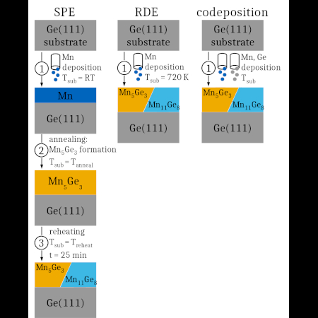
Tuning the Mn5Ge3 and Mn11Ge8 thin films phase formation on Ge(111) via growth process
Mohamed-Amine Guerboukha, Matthieu Petit, Aurélie Spiesser, Alain Portavoce, Omar Abbes, Vasile Heresanu, Sylvain Bertaina, Cyril Coudreau, Lisa Michez
Thin Solid Films 761:139523 (2022)10.1016/j.tsf.2022.139523
Control of Oxygen Vacancy Ordering in Brownmillerite Thin Films via Ionic Liquid Gating
Hyeon Han, Arpit Sharma, Holger Meyerheim, Jiho Yoon, Hakan Deniz, Kun-Rok Jeon, Ankit Sharma, Katayoon Mohseni, Charles Guillemard, Manuel Valvidares, Pierluigi Gargiani, Stuart Parkin
ACS Nano 16:6206-6214 (2022)10.1021/acsnano.2c00012
Reversal of Anomalous Hall Effect and Octahedral Tilting in SrRuO3 Thin Films via Hydrogen Spillover
Hyeon Han, Hua Zhou, Charles Guillemard, Manuel Valvidares, Arpit Sharma, Yan Li, Ankit Sharma, Ilya Kostanovskiy, Arthur Ernst, Stuart Parkin
Advanced Materials 35 (2022)10.1002/adma.202207246
Highly ordered carbon penetration into the Mn5Ge3Cx lattice: A superstructure in Mn5Ge3C0.5 inferred from a Mn55 NMR study
R. Kalvig, E. Jedryka, M. Wojcik, M. Petit, L. Michez
Physical Review B 105:094405 (2022)10.1103/PhysRevB.105.094405
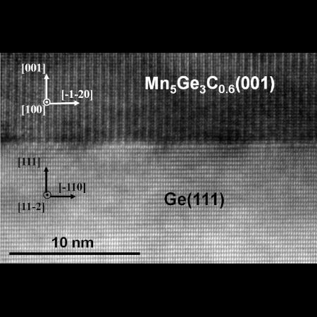
Unveiling the atomic position of C in Mn5Ge3Cx thin films
L.-A. Michez, M. Petit, V. Heresanu, V. Le Thanh, E. Prestat, F. d'Acapito, Q. Ramasse, F. Boscherini, P. Pochet, M. Jamet
Physical Review Materials 6:074404 (2022)10.1103/PhysRevMaterials.6.074404
XPS modeling of GaN/GaAs nanostructure grown by the droplet epitaxy technique
Guy Tsamo, Guillaume Monier, Philip Hoggan, Christine Robert-Goumet, Matthieu Petit, Alain Ranguis, Luc Bideux
Journal of Electron Spectroscopy and Related Phenomena 261 (2022)10.1016/j.elspec.2022.147257
2021
Nanocontact vortex oscillators based on Co$_2$MnGe pseudo spin valves
Jérémy Létang, Claudia de Melo, Charles Guillemard, Aymeric Vecchiola, Damien Rontani, S. Petit-Watelot, Myoung-Woo Yoo, Thibaut Devolder, Karim Bouzehouane, Vincent Cros, Stéphane Andrieu, Joo-Von Kim
Physical Review B 103:224424 (2021)10.1103/PhysRevB.103.224424
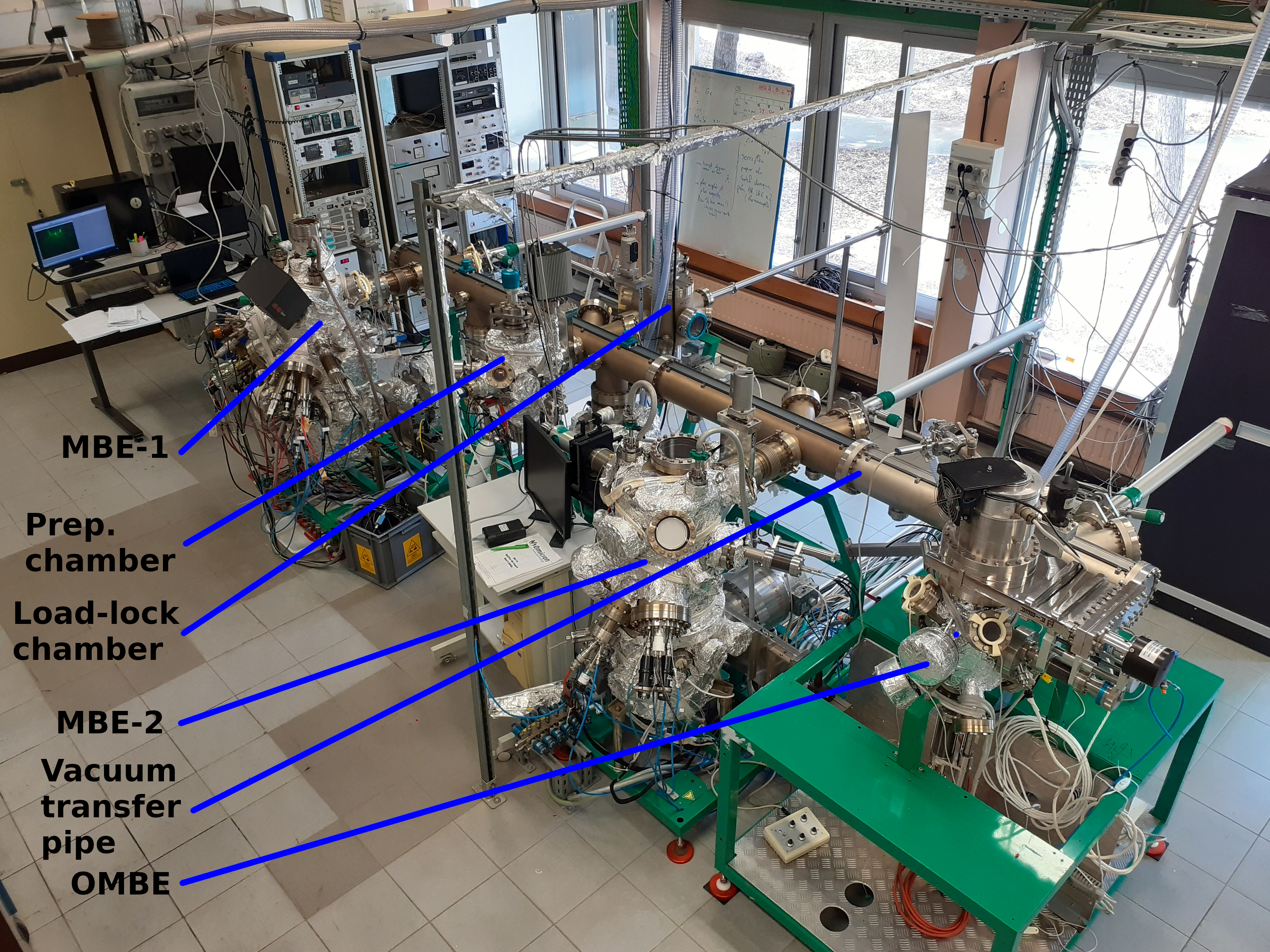
UHV equipment for spintronic applications
Ultrahigh vacuum (UHV) growth system dedicated to Ge/Si-based heterostructures for spintronic applications:
- A load-lock chamber equipped with a 4 samples holder carousel
- The main Molecular Beam Epitaxy (MBE) growth chambers:
- MBE-1: Si, Ge, P, C, Al, Mn
- MBE-2: metals (Au, Cr, Co, Mn, Ru, Sn etc)
- OMBE: organic molecules (PTCDI, etc)
- a preparation chamber (ionic cleaning)
- A 4 meters long vacuum transfer pipe connecting these three chambers allowing samples transfers without air exposure.
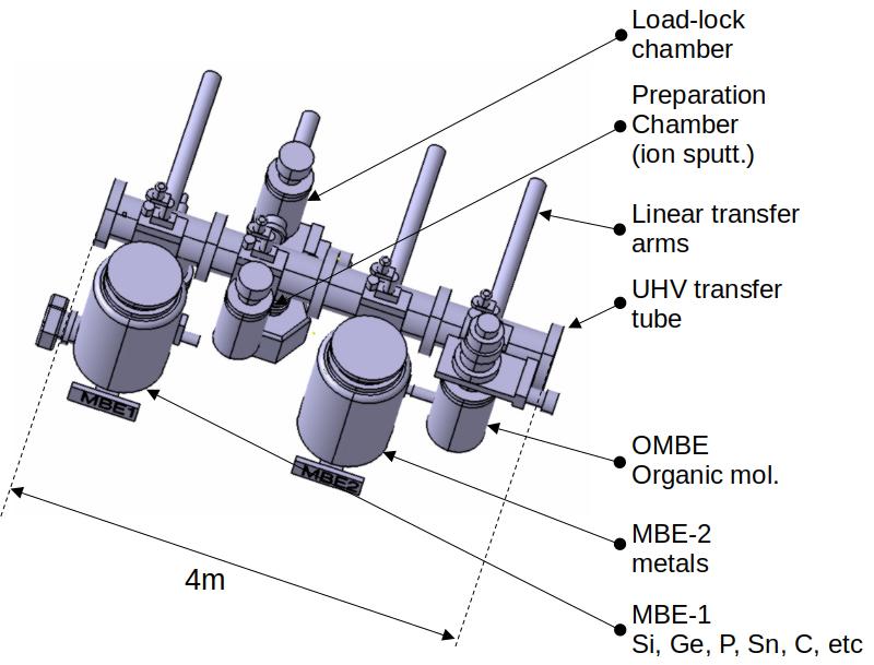
The maximum size of the samples which can be used is 5 cm / 2” in diameter.
The sample holders can be heated up to 1100°C.
We also have:
- a UHV suitcase to transfer samples
- an Omicron-type sample plates / molyblock adaptator
Effusion and sublimation cells are installed in the MBE chambers:
- Ge, Mn, Sb, Au
- Doping cells: Si, C, GaP (P) (SUSI-D, SUKO-D and DECO-D sources respectively, from MBE-Komponenten)
The growth processes and thin films can be characterized in situ by:
- quartz crystal microbalance
- RHEED (Reflection high-energy electron diffraction)
- AES (Auger electrons spectroscopy)
National
- IM2NP, Marseille
- CEA, Orsay
- SPINTEC, Grenoble
- Institut Néel, Grenoble
- Institut Pascal, Clermont-Ferrand
- C2N, Paris
International
- IFPAN, Varsaw, Poland
- AIST, Tsukuba (つくば市), Japan
- University of Stuttgart, Stuttgart, Germany
- University of Manchester, UK