Nanomaterials
Discovering, processing and assembling (new) materials allowed to set landmarks in the evolution of humankind, society and technology since pre-historical times. This holds especially true nowadays in the era of (opto)electronics, that owes to the fine control of materials at the nanoscale its success. The synthesis of nanoscale materials with controlled physical and chemical properties can enable profound advances in science and technology. In the group we investigate the fundamental benefits of finely manipulating nanocrystals at different scales to make the bottom-up realisation of complex 3D monocrystalline nano-architectures for optoelectronics a reality. In particular we focus on the following aspects:
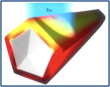
Nanomaterial synthesis. Our core expertise is the development of new synthetic techniques to achieve high-quality nanoscale materials, in particular via solution processes. We are especially interested in single-crystalline materials, such as nanowires and nanocubes and core-shell heterostructures, that we can synthesize for various material compositions (metallic, semiconducting and insulating).
Nanomaterial assembly. The capability of controlling the position of individual nanocrystals with precision on a large scale is key to bridging the gap between top-down and bottom-up approaches. We employ directed assembly techniques to immobilize colloidal nanocrystals in templates with nanopatterned recessions. The obtained 2D nanopattern is then printed to a new substrate, for example to integrate a metasurface on optoelectronic devices. With the ambition to take this approach to the limit we are currently investigating strategies to improve the yield of assembly and printing to obtain a defect-free nanopattern.
Characterisation of nanostructures. We use state of the art techniques to characaterise structural, optical, chemical and electrical properties of newly synthesized nanoscale materials at the individual level and at the ensemble level. This allows to shine light on the fundamental properties and identify routes to improve performance.
Selected Publications
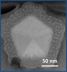
B. Sciacca, A. Berkhout, B. J. M. Brenny, S. Z. Oener, M. A. van Huis, A. Polman, E. C. Garnett
Monocrystalline Nanopatterns Made by Nanocube Assembly and Epitaxy
Advanced Materials 29, 1701064 (2017) ➡ pdfS. A. Mann, B. Sciacca, Y. Y. Zhang, J. Wang, E. Kontoleta, H. Y. Liu, E. C. Garnett
Integrating Sphere Microscopy for Direct Absorption Measurements of Single Nanostructures
Acs Nano 11, 1412 (2017) ➡ pdfB. Sciacca, J. van de Groep, A. Polman, E. C. Garnett
Solution-Grown Silver Nanowire Ordered Arrays as Transparent Electrodes
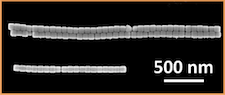
Advanced Materials 28, 905 (2016) ➡ pdfB. Sciacca, A. O. Yalcin, E. C. Garnett
Transformation of Ag Nanowires into Semiconducting AgFeS2 Nanowires
Journal of the American Chemical Society 137, 4340 (2015) ➡ pdfB. Sciacca, S. A. Mann, F. D. Tichelaar, H. W. Zandbergen, M. A. van Huis, E. C. Garnett
Solution-Phase Epitaxial Growth of Quasi-Monocrystalline Cuprous Oxide on Metal Nanowires
Nano Letters 14, 5891 (2014) ➡ pdf