Optoelectronic devices
Electronic and optoelectronic devices are ubiquitous components in our daily life, and impact many areas of society, such solar cells or LEDs. New technologies or strategies, that can provide bettwer efficiencies at reduced costs, are needed to tackle the energy challenge. Quality of the materials (monocrystalline, low non-radiative recombinations), quality of the interfaces (passivation, low non-radiative recombinations) and light-matter interactions (light trapping, directional emission) are the main ingredients to achieve efficiencies close to the thermodynamical limit. Simple fabrication procedure and low material cost (earth abundant, nanostructured) are the main ingredients to reduce costs. Operating at the nanoscale offers the unique opportunity to meet these requirements. In the group we investigate the fundamental benefits of finely manipulating nanocrystals at different scales to make the bottom-up realisation of complex 3D monocrystalline nano-architectures for optoelectronics a reality. In particular we focus on the following aspects:
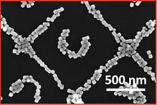
Metasurfaces. We investigate the advantages of using complex core-shell nanostructures, with a tailored dielectic function, as building blocks for the realization of metasurfaces on a large scale, that can be printed on any substrate. In particular, we are study metasurfaces to reduce the entropic losses of solar cells due to light emission.
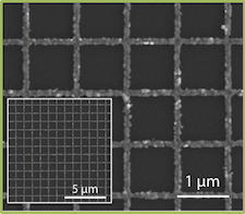
Transparent electrodes. We already have shown that nanowire-based transparent electrodes outperform standard approahces bases on conductive metal oxides. We are taking this approach one step further and are working on the realisation of monocrystalline nanowire networks transparent electrode, fully solution processed at low temperature. This will allow to achieve ultimate performance and will find application in many optoelectronic devices.
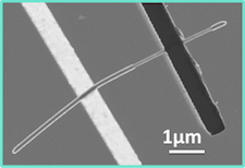
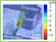
Nanoscale solar cells. The study of nanoscale solar cells allows to gain unvaluable understanding of fundamental processes that are disguised and difficult to unveil in macroscopic solar cells. We investigate photon absorption due to optical resonance, radiative and non-radiative carrier recombination the role of interfaces in electron transfer in individual nanostructured devices. This will allow to come up with better solutions to improve performance.
Selected Publications
S. H. Gong, F. Alpeggiani, B. Sciacca, E. C. Garnett, L. Kuipers
Nanoscale chiral valley-photon interface through optical spin-orbit coupling
Science 359, 51 (2018) ➡ pdfX. Z. Zheng, B. Sciacca, E. C. Garnett, L. W. Zhang
AgFeS2-Nanowire-Modified BiVO4 Photoanodes for Photoelectrochemical Water Splitting
ChemPlusChem 81, 1075 (2016) ➡ pdfB. Sciacca, J. van de Groep, A. Polman, E. C. Garnett
Solution-Grown Silver Nanowire Ordered Arrays as Transparent Electrodes
Advanced Materials 28, 905 (2016) ➡ pdfS. Z. Oener, S. A. Mann, B. Sciacca, C. Sfiligoj, J. Hoang, E. C. Garnett
Au-Cu2O core-shell nanowire photovoltaics
Applied Physics Letters 106, 023501 (2015) ➡ pdf