News
 |
03.2024
We are looking for candidates for two funded PhD projects: Please do not hesitate to contact us! |
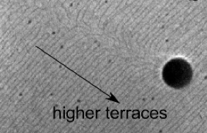
Tiré de Adv. in Phys. 41 (1992) 59


2026
The Submerged Pre‐Columbian Site of Fond Banane (Martinique, French West Indies): Insights Into Late Holocene Coastal Dynamics and Human–Environment Interactions on the Edge of the Mangroves
Morgane Blanot, F. Leroy, B. Bérard, F. Dolique, C. Morhange, D. Delanghe, S. Lebarillier, P. Wong Wah Chung
Geoarchaeology: An International Journal 41:e70047 (2026)10.1002/gea.70047
Growth and domain structure of GeTe ferroelectric thin films on miscut silicon substrates: The key role of atomic steps
Léa Meynier, Fabio Verducci, Guillaume Ayala, Boris Croes, Fabien Cheynis, Pierre Müller, Stefano Curiotto, Salia Cherifi-Hertel, Frédéric Leroy
Journal of Applied Physics 139 (2026)10.1063/5.0280904
Spin texture of α−GeTe in the ultrathin regime
Calvin Tagne-Kaegom, Alexandre Llopez, Boris Croes, Geoffroy Kremer, Bertrand Kierren, Daniel Malterre, Luc Moreau, Fotié Jaurès Ngoufo, Stefano Curiotto, Pierre Müller, Patrick Le Fèvre, Julien Rault, François Bertran, Andrés Saúl, Frédéric Leroy, Fabien Cheynis, Yannick Fagot-Revurat
Physical Review B 113:125113 (2026)10.1103/yst7-ktp9
2025
Thermomigration of Au-Ge microdroplets on Ge(111): Atomic mechanisms and effects on surface morphology
Nayef Abu Dahech, Frédéric Leroy, Pierre Müller, Fabien Cheynis, Stefano Curiotto
Physical Review Materials 9:103403 (2025)10.1103/p1lf-r9y9
Real-time helium bubble growth in tungsten by in-situ GISAXS
L. Corso, S. Curiotto, F. Cheynis, P. Muller, Elodie Bernard, M. Cabie, C. Martin, F. Leroy
Nuclear Materials and Energy 42:101894 (2025)10.1016/j.nme.2025.101894
A combined 2ω/3ω method for the measurement of the in-plane thermal conductivity of thin films in multilayer stacks: Application to a silicon-on-insulator wafer
F. Mazzelli, J. Paterson, F. Leroy, O. Bourgeois
Journal of Applied Physics 137:015106 (2025)10.1063/5.0227482
2024
Polarization structure of nanostrip domain intersections in GeTe films
Boris Croes, Fabien Cheynis, Salia Cherifi Cherifi-Hertel, Kokou Dodzi Dorkenoo, Pierre Müller, Stefano Curiotto, Frédéric Leroy
Physical Review B 109:024103 (2024)10.1103/PhysRevB.109.024103
Pushing the thickness limit of the giant Rashba effect in ferroelectric semiconductor GeTe
Boris Croes, Alexandre Llopez, Calvin Tagne-Kaegom, Bodry Tegomo Chiogo, Bertrand Kierren, Pierre Müller, Stefano Curiotto, Patrick Le Fèvre, François Bertran, Andrés Saúl, Yannick Fagot-Revurat, Frédéric Leroy, Fabien Cheynis
Nano Letters (2024)10.1021/acs.nanolett.4c03281
Rim nucleation and step-train orientation effects in SOI(111) dewetting
Stefano Curiotto, Pierre Müller, Fabien Cheynis, Igor Ozerov, Frédéric Leroy
Surfaces and Interfaces 45:103912 (2024)10.1016/j.surfin.2024.103912
Surface thermomigration of 2D voids
Stefano Curiotto, Nicolas Combe, Pierre Müller, Ali El Barraj, Nayef Abu Dahech, Fabien Cheynis, Olivier Pierre-Louis, Frédéric Leroy
Applied Physics Letters 125:121601 (2024)10.1063/5.0228961
Van der Waals epitaxy of Weyl-semimetal Td-WTe2
Alexandre Llopez, Frédéric Leroy, Calvin Tagne-Kaegom, Boris Croes, Adrien Michon, Chiara Mastropasqua, Mohamed Al Khalfioui, Stefano Curiotto, Pierre Müller, Andrés Saúl, Bertrand Kierren, Geoffroy Kremer, Patrick Le Fèvre, François Bertran, Yannick Fagot-Revurat, Fabien Cheynis
ACS Applied Materials & Interfaces 16:20878-20885 (2024)10.1021/acsami.4c00676
2023
Tungsten evolution under helium irradiation: Shape of bubbles by TEM and in-situ GISAXS analysis
L. Corso, S. Curiotto, E. Bernard, Martiane Cabie, C. Martin, Lucio Martinelli, Fabien Cheynis, Pierre Müller, Frédéric Leroy
Nuclear Materials and Energy 37:101533 (2023)10.1016/j.nme.2023.101533
Early-stage growth of GeTe on Si(111)-Sb
Boris Croes, Fabien Cheynis, Yannick Fagot-Revurat, Pierre Müller, Stefano Curiotto, Frédéric Leroy
Physical Review Materials 7:014409 (2023)10.1103/PhysRevMaterials.7.014409
Thermomechanic behavior of epitaxial GeTe ferroelectric films on Si(111)
Boris Croes, Fabien Cheynis, Michaël Texier, Pierre Müller, Stefano Curiotto, Frédéric Leroy
Journal of Applied Physics 134:204103 (2023)10.1063/5.0173718
Atomistic Description of Interdroplet Ice-Bridge Formation during Condensation Frosting
Stefano Curiotto, David Paulovics, Christophe Raufaste, Franck Celestini, Thomas Frisch, Frédéric Leroy, Fabien Cheynis, Pierre Müller
Langmuir 39:579 (2023)10.1021/acs.langmuir.2c02860
Size-dependent diffusion of 3D nanovoids in a bcc solid
Stefano Curiotto, Pierre Müller, Fabien Cheynis, Loic Corso, Elodie Bernard, Frédéric Leroy
Applied Physics Letters 123:241603 (2023)10.1063/5.0175752
2022
Polar surface of ferroelectric nanodomains in GeTe thin films
B. Croes, F. Cheynis, P. Müller, S. Curiotto, F. Leroy
Physical Review Materials 6:064407 (2022)10.1103/PhysRevMaterials.6.064407
Automatic Ferroelectric Domain Pattern Recognition Based on the Analysis of Localized Nonlinear Optical Responses Assisted by Machine Learning
Boris Croes, Iaroslav Gaponenko, Cédric Voulot, Olivier Grégut, Kokou D Dorkenoo, Fabien Cheynis, Stefano Curiotto, Pierre Müller, Frédéric Leroy, Kumara Cordero‐edwards, Patrycja Paruch, Salia Cherifi Cherifi-Hertel
Advanced Physics Research 2200037 (2022)10.1002/apxr.202200037
Hole opening from growing interfacial voids: A possible mechanism of solid state dewetting
Stefano Curiotto, Anna Chame, Pierre Müller, Carl Thompson, Olivier Pierre-Louis
Applied Physics Letters 120:091603 (2022)10.1063/5.0083139
Reflections on the effect of an external flux in surface physics
Stefano Curiotto, F. Leroy, F. Cheynis, P. Müller
Surface Science : A Journal Devoted to the Physics and Chemistry of Interfaces 725:122158 (2022)10.1016/j.susc.2022.122158
2021
Kinetic Monte Carlo simulations of the diffusion and shape evolution of single-layer clusters on a hexagonal lattice with and without external force
Stefano Curiotto, Pierre Müller, Fabien Cheynis, Frédéric Leroy
Applied Surface Science 552:149454 (2021)10.1016/j.apsusc.2021.149454
Mechanism of droplet motion and in-plane nanowire formation with and without electromigration
Stefano Curiotto, Pierre Müller, Fabien Cheynis, Frédéric Leroy
Applied Surface Science 579:152015 (2021)10.1016/j.apsusc.2021.152015
2020
2D Manipulation of Nanoobjects by Perpendicular Electric Fields: Implications for Nanofabrication
Stefano Curiotto, F. Cheynis, Pierre Müller, Frédéric Leroy
ACS Applied Nano Materials 3:1118-1122 (2020)10.1021/acsanm.9b02517
Magnetic anisotropy of one-dimensional Co nanostructures
Michel Daher Mansour, Romain Parret, F. Cheynis, Matthieu Petit, Fadi Choueikani, Lisa Michez, Laurence Masson
Physical Review B 102:155403 (2020)10.1103/PhysRevB.102.155403
Dynamics of Au-Ge liquid droplets on Ge(1 1 1) terraces: Nucleation, growth and dynamic coalescence
Ali El-Barraj, Stefano Curiotto, Fabien Cheynis, Pierre Müller, Frédéric Leroy
Applied Surface Science 509:144667 (2020)10.1016/j.apsusc.2019.144667
Dynamics of Gold Droplet Formation on SiO 2 /Si(111) Surface
Hadi Hijazi, Frédéric Leroy, Guillaume Monier, Gabin Grégoire, Evelyne Gil, Agnès Trassoudaine, Vladimir G Dubrovskii, Dominique Castelluci, Nebile Isik Goktas, Ray Lapierre, Yamina André, Christine Robert-Goumet
Journal of Physical Chemistry C 124:11946-11951 (2020)10.1021/acs.jpcc.0c02378
Electric forces on a confined advacancy island
Frédéric Leroy, Ali El-Barraj, Fabien Cheynis, Pierre Müller, Stefano Curiotto
Physical Review B 102 (2020)10.1103/PhysRevB.102.235412
Kinetics and coupled dynamics of dewetting and chemical reaction in Si/SiO2/Si system
Frédéric Leroy, D Landru, Fabien Cheynis, O Kononchuk, Pierre Müller, Stefano Curiotto
Journal of Materials Science (2020)10.1007/s10853-020-05161-w
Nanomateriaux Structure, morphologie et stabilite
Pierre Müller
Techniques de l’Ingénieur. Techniques d'Analyse NM3010 (2020)
Propriétés des nano-objets: Longueurs critiques, effets de taille et de forme
Pierre Müller
Techniques de l’Ingénieur. Techniques d'Analyse (2020)

-
2023-2027 : HEBUTERNE Project (ANR-23-CE08 - PRC)
Helium Bubble formation in Tungsten: from Nanoscience understanding to macroscale impact
(Coordinateur : E. Bernard, CEA/IRFM) -
2022-2026 : Projet FETh ( ANR-22-CE08 - PRC)
Ferroelectric control of nanoscale Electric and Thermal conduction in GeTe
(Coordinateur: F. Leroy) -
2022-2026 : Projet Thermotweez (ANR-22-CE09 - PRME)
Déplacement de nanostructures de surface contrôlé par thermomigration
(Coordinateur: S. Curiotto) -
ANR Project 2DTransformers (ANR-14-OHRI-0004)
-
ANR Project HoloLEEM (ANR-15-CE09-0012)
-
ANR Project LOTUS (ANR-13-BS04-0004-02)
![]()
-
2024-2028 : Projet HIBERNIA
Helium bubbles in plasma-facing material of fusion reactors: a nanoscience
approach
(Coordinateur: F. Leroy) -
2023-2027 : Projet FRICTION
Ferroelectric Rashba semiconductors for spin orbitronics
(Coordinateur: F. Cheynis) -
2023-2027 : Projet INDIGENA
Interfacial Design of Optical High-Harmonic Generation
(Coordinateur: C. Attaccalite, CINaM)
Aix-Marseille Univ. collaborations
- O. M. Texier & O. Thomas (IM2NP, Marseille)
- C. Martin (PIIM, Marseille)
French Collaborations
-
- O. Pierre-Louis (ILM, Lyon)
- E. Bernard (CEA/IRFM, Saint Paul-lez-Durance)
- S. Cherifi-Hertel (IPCMS, Strasbourg)
- Y. Fagot-Revurat, B. Kierren & D. Malterre (Institut Jean Lamour, Nancy)
- A. Michon, M. Al Khalfioui & M. Portail (CRHEA, Valbonne)
- J.-P. Attané & L. Vila (CEA/SPINTEC, Grenoble)
- J. Coraux (Institut Néel, Grenoble)
- L. Martinelli & G. Renaud (ESRF, beamline BM32, Grenoble)
International collaborations
- B. Ranguelov & M. Michailov (IPC, BAS, Bulgary)
- Y. Saito (Keio Univ., Japan)
- C. V. Thompson (MIT, Cambridge, USA)
-
Method for making semi-conductor nanocrystals (Nov. 8, 2012)
Ł. Borowik, J.-C. Barbé, E. Bussmann, F. Cheynis, F. Leroy, D. Mariolle and P. Müller. Publication Number: US2012282758.
Ł. Borowik, J.-C. Barbé, E. Bussmann, F. Cheynis, F. Leroy, D. Mariolle and P. Müller. Publication Number: US2012282759.
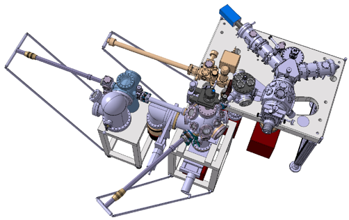
UHV set-up @ CINaM
On a daily basis, we use a UHV experimental set dedicated to surface physics, including a LEEM/PEEM microscope [1,2], a STM/AFM microscope [3,4] and a surface preparation chamber. An overview of the equipment can be seen below. The LEEM microscopy technique enables us to visualize and film crystalline surfaces (typical acquisition time 0.1-1s) in a UHV environment (a few 10-10 Torr or typ. 10-13 bar) or under a partial pressure (a few 10-7 Torr : H2, N2, O2, ...) at high temperatures (≈1300K)or below room temperature (≈150K).
this technique is therefore particularly well suited to in-situ, real-time characterization of crystalline surfaces and thin films on a mesoscopic scale (field of view: a few 1µm to 50µm with a typical lateral resolution of 5nm and a vertical atomic resolution).
In diffraction mode, this equipment can acquire LEED (Low-Energy Electron Diffraction) images, enabling to determine the atomic structure of the imaged surface. As with transmission electron microscopy (TEM), LEEM microscopy enables both bright-field and dark-field imaging of the surface to be characterized. This makes it possible to distinguish regions with different atomic arrangements on the surface.
A full description of the instrumental set-up can be found in the following reference: Rev. Sci. Instr. 85 (2014) 043705
Examples of LEEM images obtained with our microscope are available below.
Left: Si(001) surface at 1000°C in dark field. The white-black contrast results from the difference in crystallographic structure between adjacent atomic terraces in the case of Si(001) (field of view: 15µm). A film illustrating the sublimation of the silicon surface at high temperatures is also available here.
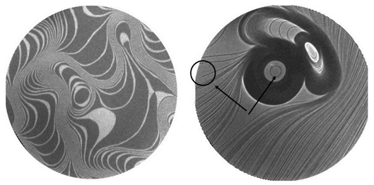
Right: Mo(110) surface at 1070°C in bright-field mode. The contrast used to visualize atomic steps (black lines) is due to the phase difference between electron waves scattered by two terraces separating a step. The black circle indicates a screw dislocation emerging from the crystal surface, and the black arrow indicates a circular atomic step at the top of a circular pyramid (field of view: 7.5µm).
Nanofabrication @PLANETE (CINaM)
Nanoscience research frequently relies on the use of artificially structured samples on the nanometric scale. For this reason, we are regular users of the nanofabrication platform PLANETE at CINaM. More specifically, our scientific projects require the use of clean-room technology processes such as :
- Chemical cleaning
- Optical and/or electronic lithography
- Plasma etching
Characterization techniques and Synchrotron facilities
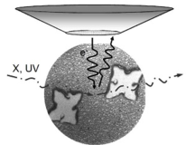
For a detailed understanding of the relationships between atomic structure, surface dynamics and electronic properties, characterizations complementary to those available in our experimental set are generally required. Surface characterization techniques based on synchrotron radiation offer the possibility of combining real-space and reciprocal-space approaches. Here is a short (and non-exhaustive!) list of the techniques we regularly use:
- Grazing Incidence X-ray diffraction (GIXD) & Grazing Incidence Small-Angles X-ray scattering (GISAXS) @BM32 (ESRF)
- Angle-resolved photoemission spectroscopy (ARPES) @CASSIOPEE (SOLEIL)
- Spectromicroscopy XPEEM @HERMES (SOLEIL), @Nanospectroscopy (ELETTRA)
Electromigration of Au on Ge(111)
2D Au islands (dark grey) detach from step edges and migrate in the direction opposite to the current. Temperature: 500°C. Field of view: 6.5x4.5µm2. Time: 4min. (unpublished results).
Electromigration on Si(111)
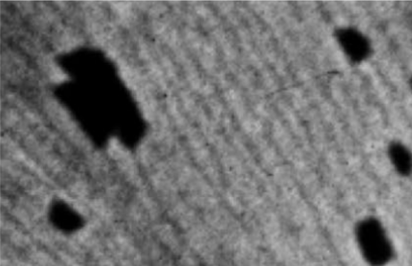
Electromigration of two single-atom deep holes (dark grey) on a Si(111)-7x7 terrace (light grey). They migrate in the direction opposite to the electric current (that is reversed twice). The holes are in a metastable Si(111)-(1x1) surface reconstruction. Field of view: 28x12µm2. Temperature ≤830°C. Time: 35min (unpublished results).
Electromigration on Si(100)
Single-atom deep holes (black ellipses) move under the effect of an electric current. The current direction is from left to right. The sample temperature is at 1170K, the window width is 18µm and the real-time experiment duration is 9 minutes. Appl. Surf. Sci., 469, 463 (2019).
2D elec. gas induced by a Ag deposition
At ε=24 eV, the image shows the Ag adatom concentration variations. At ε=1.8 eV, the LEEM image illustrates qualitatively the surface work function time evolution (i.e. the 2DEG doping). Sci. Rep. 7 (2017) 10642.
Dewetting of a Si(100) film on a SiO2 substrate
The black-white regions at the top of the imaged area are Si(100) terraces with 2x1 or 1x2 surface reconstruction. The dewetting front advances and when O2 is introduced in the chamber it stops. The Si terraces alternatively blink between white and black during O2 exposure because Si is consumed according to the reaction Si+1/2O2=SiO(gas). The sample temperature is 1100K.
Au-Si droplets moving on Si(111)
The droplets climb up and locally dissolve the Si steps (field-of-view: 10µm).
Surface phase transformation on Si(111)
White and dark regions are 7x7 and 1x1 surface phases respectively. Below 830ºC the 7x7 phase is stable with a small amount of residual, metastable 1x1. Upon heating the sample above 830ºC, the 7x7 phase reduces and disappears while the 1x1 domains widen. Decreasing the temperature below 830ºC, the 7x7 domains nucleate and grow. The process is reversible. The window width is 7µm.